Forwarding 5 Stage CPU

Introduction
In this project, I developed a five-stage pipelined CPU using Verilog. The design was focused on implementing a MIPS-based architecture with integrated forwarding to efficiently handle data hazards. Pipelining is a technique used in CPU design to increase instruction throughput by overlapping the execution of multiple instructions. This project aimed to explore and implement the key stages of a CPU pipeline: Instruction Fetch (IF), Instruction Decode (ID), Execute (EX), Memory Access (MEM), and Writeback (WB).
The CPU was designed to process instructions sequentially while minimizing delays caused by data dependencies between instructions. By integrating forwarding mechanisms, the CPU was able to pass results directly from one pipeline stage to another, reducing the need for stalls and improving performance. This project not only highlights the practical aspects of CPU design but also demonstrates the effectiveness of pipelining and hazard management in modern processors.
The Architecture
.png)
The above picture illustrated the 5 stages of the pipeline CPU. Starting with the first stage, IF, which fetched the MIPS instructions from instruction memory to be run. The next stage was the ID stage, where the instruction was read to determine the execution that should occur in the ALU, and the control signals were updated accordingly. At this stage, the register values were retrieved from register memory, but a multiplexer was also added to allow forwarding within the CPU. Writing back to registers only occurred at the negative edge of the clock cycle. It was also at this stage that the immediate value was extended.
The next stage of the CPU was the execute stage, where the ALU ran and performed the needed operations. At this stage, addition, subtraction, XOR, and other operations were executed. This was the stage where the actual values were calculated.
Depending on whether the control signal m2reg or mwmem was activated, the MEM stage would either load from memory, store to memory, or do neither based on the ALU value.
The last stage, Writeback, occurred where the values were written to the registers within register memory. This always occurred and was dependent on control signals.
This form of architecture benefited from a higher clock speed as the process was separated into stages, allowing each stage to run in less time than if all instructions ran at once. This architecture also had greater throughput of instructions since an instruction didn’t have to wait for the previous one to finish before it could start. The format also allowed for simplification, as each step could be optimized separately, with the stages being clearly defined. This enabled teams to work on different stages, like IF and ID, independently. Once both teams were finished, they could potentially improve the clock speed of the product as a whole.
Implementation
The development of this five-stage pipelined CPU was carried out in Verilog, with a focus on modular design. Each stage of the pipeline—Instruction Fetch (IF), Instruction Decode (ID), Execute (EX), Memory Access (MEM), and Writeback (WB)—was implemented as a separate module. These modules were then integrated to form the complete CPU, with careful attention paid to the connections and data flow between stages.
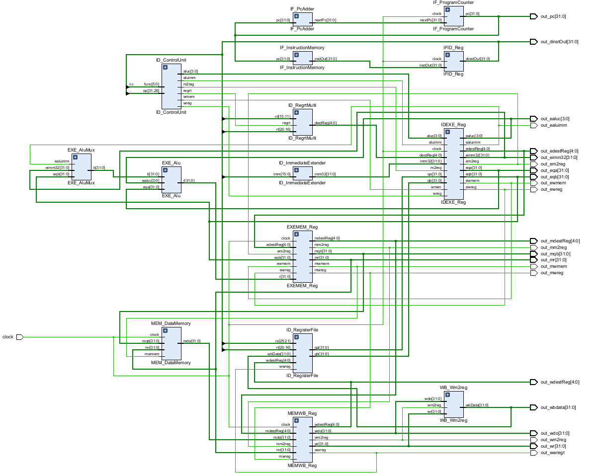
Below is a graphical representation of the schematic of the final CPU:

This schematic illustrates the modular nature of the design, where each block represents a distinct stage of the CPU pipeline. The lines between modules represent the connections, implemented with wires, that allow for the transfer of data and control signals throughout the pipeline.
To ensure proper functionality, an I/O planning diagram was developed and implemented. This diagram details the input and output signals for each module, ensuring that data is correctly routed and that control signals are properly managed.
The I/O planning was crucial in the integration phase, ensuring that all components communicated effectively and that the CPU operated as intended. This methodical approach to design and integration enabled the successful implementation of the CPU, capable of executing a range of MIPS instructions with minimal delay and high efficiency.
Conclusion
In this project, the forwarding integrated CPU was successfully implemented and verified using a series of MIPS instructions. Below is a sequence of instructions that the CPU executed:
assign rom[6'h00] = 32'h00221820; // (00) add $3, $1, $2
assign rom[6'h01] = 32'h01232022; // (00) sub $4, $9, $3
assign rom[6'h02] = 32'h00692825; // (00) or $5, $3, $9
assign rom[6'h03] = 32'h00693026; // (00) xor $6, $3, $9
assign rom[6'h04] = 32'h00693824; // (00) and $7, $3, $9
The CPU was able to run these instructions back-to-back without stalling, thanks to the forwarding mechanism that allowed intermediate results to be passed directly between pipeline stages. For example, the result of the add instruction (add $3, $1, $2) was immediately forwarded to the subsequent sub instruction (sub $4, $9, $3), without waiting for the add instruction to complete fully through the pipeline.
This efficient handling of data hazards was further evidenced in the waveform below, which shows the signal states as the instructions were processed:
The waveform illustrates the timing and control signals at various stages of the pipeline, demonstrating the correct functioning of the CPU as it processed each instruction in sequence. The successful execution of these instructions confirms the effectiveness of the forwarding integrated CPU design, achieving higher instruction throughput and better overall performance.

